350 nm is massive and ancient relative to new processes, but the name of a new process stopped physically meaning anything a while ago. for instance, the 3 nm process smallest distance between traces is only 24 nm.
now the industry just names a new process when enough techniques for improving performance (without much actual size difference) exist.
breaking taps is very impressive, but sam zeloof made it quite a bit further, he made his own packaged IC. now he runs a startup called atomic semi, that is trying to use electron beam lithography for prototyping.
Not a guide missile with any kind of scrambling necessary to not get obliterated by current DoD tech. When it comes to realtime, clock-rate is everything.


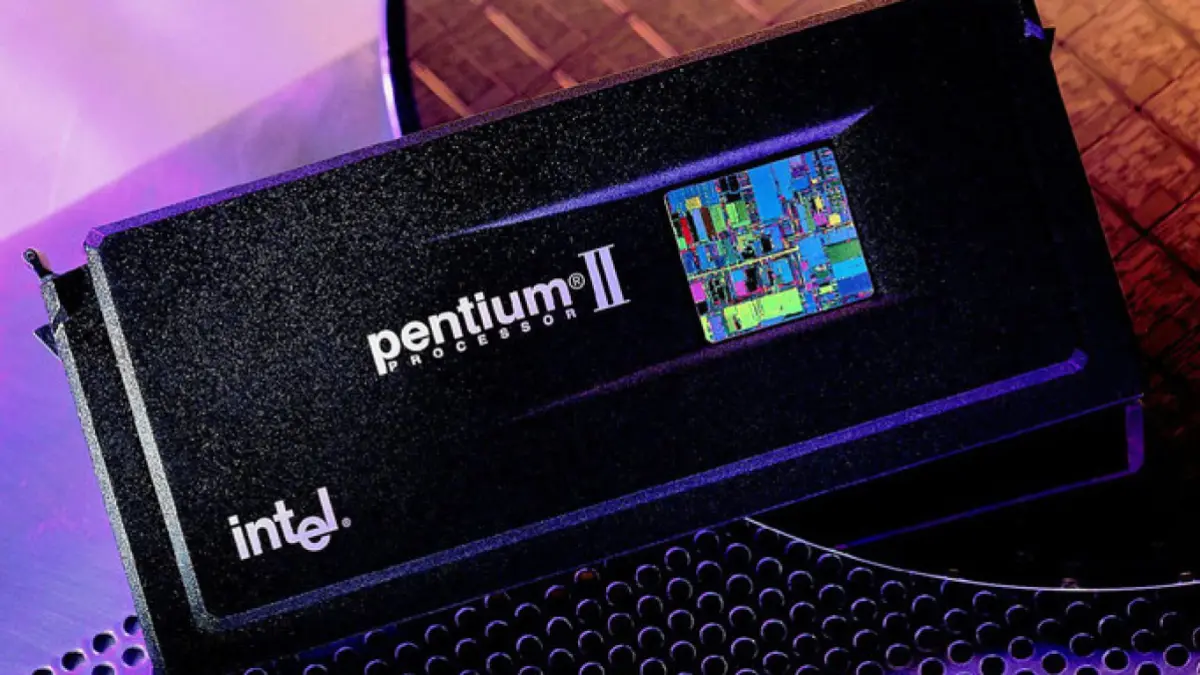
The 350 nanometer process is a level of semiconductor process technology that was reached in the 1995–1996 timeframe
The new stuff is 3nm
350 nm is massive and ancient relative to new processes, but the name of a new process stopped physically meaning anything a while ago. for instance, the 3 nm process smallest distance between traces is only 24 nm.
now the industry just names a new process when enough techniques for improving performance (without much actual size difference) exist.
I think this youtuber might have achieved similar nm with his DIY setup, but I don’t remember. He’s using a different process though.
breaking taps is very impressive, but sam zeloof made it quite a bit further, he made his own packaged IC. now he runs a startup called atomic semi, that is trying to use electron beam lithography for prototyping.
More than enough power to guide a missile.
Not a guide missile with any kind of scrambling necessary to not get obliterated by current DoD tech. When it comes to realtime, clock-rate is everything.
A stupid missile for sure, you don’t even need a computer for that.
The newest stuff out of Taiwan is 1.6nm.
Baby steps