

- cross-posted to:
- [email protected]
- cross-posted to:
- [email protected]
You must log in or register to comment.
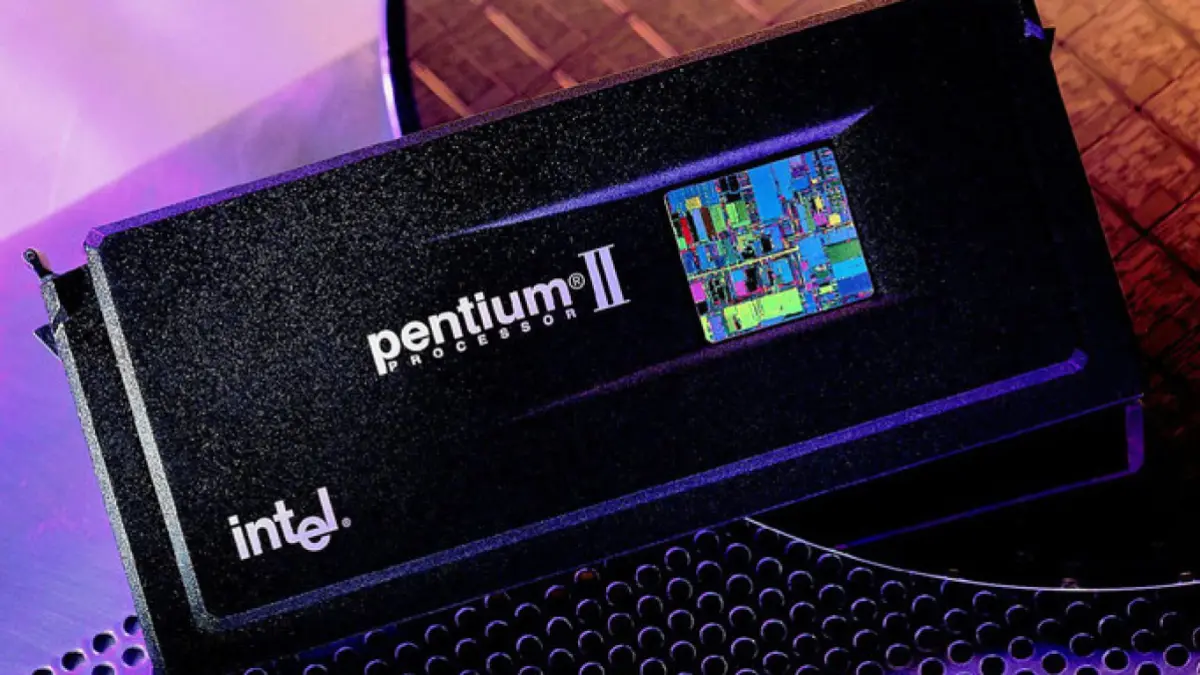
The 350 nanometer process is a level of semiconductor process technology that was reached in the 1995–1996 timeframe
The new stuff is 3nm
350 nm is massive and ancient relative to new processes, but the name of a new process stopped physically meaning anything a while ago. for instance, the 3 nm process smallest distance between traces is only 24 nm.
now the industry just names a new process when enough techniques for improving performance (without much actual size difference) exist.
I think this youtuber might have achieved similar nm with his DIY setup, but I don’t remember. He’s using a different process though.
breaking taps is very impressive, but sam zeloof made it quite a bit further, he made his own packaged IC. now he runs a startup called atomic semi, that is trying to use electron beam lithography for prototyping.
More than enough power to guide a missile.
Not a guide missile with any kind of scrambling necessary to not get obliterated by current DoD tech. When it comes to realtime, clock-rate is everything.
A stupid missile for sure, you don’t even need a computer for that.
The newest stuff out of Taiwan is 1.6nm.
Baby steps
Soon they’ll be able to run Doom.
Doom was actually a little before the 350nm era. Doom was like 386 and 486 timeframe; the first Pentium machines were being made when it was released, whereas 350nm was the Pentium Pro. So if they’re working on 350nm, they’re already ahead of Doom level hardware, hopefully.
Castle Wolfenstein seems more appropriate, in some twisted backwards way.
Russia: Sanctions aren’t doing shit, we’re actually better off without the outside world
Also Russia: Hey never mind about the toilets, let me show you how we’ve mastered Nintendo 64 technology
masteredstarted working withYes, you are correct, that’s a very relevant correction. “Soon,” they say.
Not to piss on the party, but ATmega328p chips that we use in Arduinos, if I am not incorrect, is based on 350nm process, or you just scale to that size and accept the inefficiencies. People have been doing amazing stuff with worse chips in the past. Yeah modern features in modern chips are amazing but if I was a soldier my slightly smart (Arduino standards) weapon is still a deadly weapon in my arsenal
It’s kind of an embarrassing brag, though, like saying you’re finally toilet trained. Good for you, that will help, but the rest of us are way past that.
That’s cute if you think that analogy is sufficient to make you feel better. Make no mistake I hope western weapons will turn the tide but war is messy and even if you have the most advance quality weapons, quantity unfortunately still does damage even how basic, if I have 1 million soldiers with swords and bows descend on a thousand highly advanced soldiers the battle will be intense. If the west continues to drip feed support, low level basic weaponry in abundance will counter the support. The toilet training level technology has put astronauts on the moon.
Yeah, to be clear, you’re not wrong, despite the downvotes. A basic chip is better than no chip. I don’t think it will make much difference for them, though, because when they’ve needed chips there’s China and failing that smugglers. I’s also just a machine, per the headline.
Litography technology is only the first part of the deal. You need an incredible amount of knowledge to design processors, use the technology and have a working and reliable product. Manufacturing chips is difficult, you also need to source good qualitt silicon
You are right, I am between believing Russian propaganda and thinking Russia’s resiliency, the knowledge is available and they have a key partner like China that I believe will share expertise in such archaic field, these are the same Russians that stripped washing machines for their chips so the ingenuity is there
Damn, that’s only 50x larger than what the rest of the world wants.
In three days they’ll be making 2nm chips and we’ll all be screwed
50x50 times my friend, the chips are on 2D slates, the nanometre distance is just for one side…
Edit: The distance between the transistors ofc.
GMLRS: And I took that personally
Chips is going in missiles and tanks arn’t leading edge. They kill just as effectively.
That thumbnail is beyond choice. No notes. Just … spectacular.