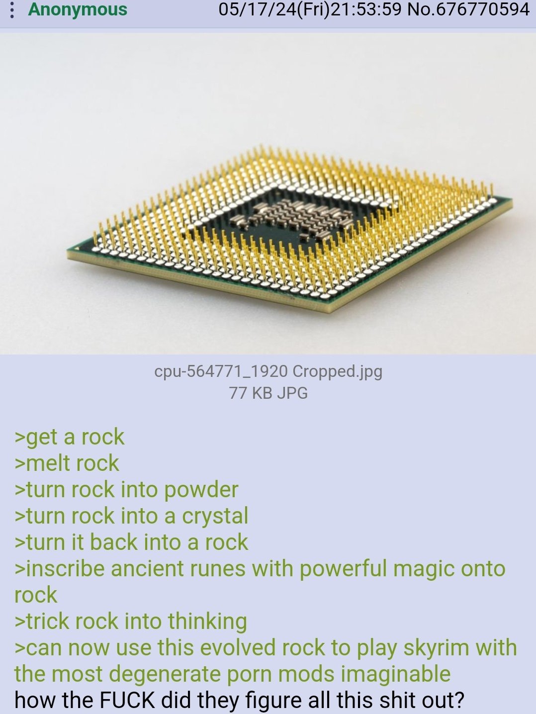
When I learned about how they are making the new CPUs it blew my mind. Dropping a microscopic droplet of metal and blasting it with lasers to a stencil like thingy to create the nanometer circuitry.
I was like how the fuck did you even thought about doing that?..
Technologies like these are really marvelous.
It’s essentially the same as somebody with a couple of cans of spray piant and a handfull of carboard sheets with cutouts spray paimting a muti-color tag on a wall.
As the logo kept getting smaller and smaller and the errors of the process of just putting that cardboard in front of the wall and spraying the whole thing had too much imperfection for tiny logos, they had to come up with more and more tricks to get it to still do tiny logos without those logos ending up too distorted.
Exactly, and “we need this as small and precise as possible” means “can lasers do it?” As an engineer I default to fast and precise means computer guided laser if possible


When I learned about how they are making the new CPUs it blew my mind. Dropping a microscopic droplet of metal and blasting it with lasers to a stencil like thingy to create the nanometer circuitry. I was like how the fuck did you even thought about doing that?.. Technologies like these are really marvelous.
You start with macroscopic photolithography, add material science of semiconductors and then iterate a million times. It didn’t start at nanoscale.
Give me a break… I’m still trying to wrap my head around how transistors work. For a layman this is like magic.
Photolithography started as a printing technique and is pretty basic.
It’s essentially the same as somebody with a couple of cans of spray piant and a handfull of carboard sheets with cutouts spray paimting a muti-color tag on a wall.
As the logo kept getting smaller and smaller and the errors of the process of just putting that cardboard in front of the wall and spraying the whole thing had too much imperfection for tiny logos, they had to come up with more and more tricks to get it to still do tiny logos without those logos ending up too distorted.
Like glueing a cardboard to the wall and then dissolving it after spraying :)
Exactly, and “we need this as small and precise as possible” means “can lasers do it?” As an engineer I default to fast and precise means computer guided laser if possible
They use electron beams and extreme UV light nowadays. Lasers are not necessarily the best light source, even at other wavelengths.