
- cross-posted to:
- [email protected]
- cross-posted to:
- [email protected]
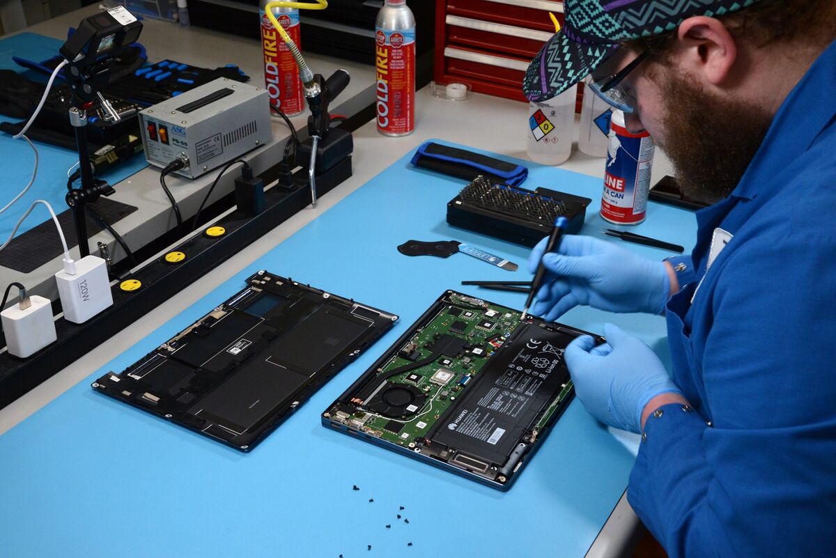
Huawei Teardown Shows 5nm Laptop Chip Made in Taiwan, Not China::Huawei Technologies Co.’s newest laptop runs on a chip made by Taiwan Semiconductor Manufacturing Co., a teardown of the device showed, quashing talk of another Chinese technological breakthrough.
Intel fab does sub 7nm. Meteor Lake processors main die use Intel 4, and the gpu die uses TSMC 5nm.
Intel’s lithography process branding is intentionally misleading:
This was done because Intel basically missed an entire generation, and AMD and Nvidia (via TSMC and Samsung) basically leapfrogged them. They’re playing catchup now, and this is marketing spin to make their stuff look better on paper by changing the numbers and removing the units so they’re not technically falsely advertising, just misleading.
Beyond the “Intel 3” node, the process names are Intel 20A and Intel 18A, which, despite the lack of hard information at the moment, I’m pretty suspicious are also misleading branding/marketing attempts, because the symbol for “angstrom” is Å, not A.
Its misleading because intel nodes at a given nm is a denser process. Finfet tech nm on its own is already a misleading number. Intels 10nm for example is a denser node than TSMCs 7nm. All companies use a non traditional method of measuring nm (as if they did, how does it make sense that a intel 10nm product have higher density than something that is “7nm”) as chip transitior is traditionally defined by the distance between transistor to transistor. And denser = transistors are closer together.
Basically intel is changing its name because its competition more or less did so, because the actual transistor distance in a traditional definition is incorrect, because finfet on its own folds over and the manufacture considers the folding technique to be a transistor when in reality its more complicated then that.
An adjacent comparison would be like treating physical cores and threads the same on a processor the same, or considering AMDs definition of a “core” during buldozer and piledriver to be the same as a traditional core (when in reality it isnt, because although there were 8 integer cores in an “8 core” processor, each pair shared one fpu) so it would challenge the definition. All fabs basically challenged the definition of what “nm” means, and theres no longer a standard to what it really means because they have all abandondoned the traditional naming scheme
Yep. I understand that. It’s still intentionally misleading.
If Intel could match the node size, they’d just call it what it is. They’re almost certainly going to catch up eventually, but this naming crap is 100% a marketing ploy. If you also consider the hilarious and asinine slide deck they put together somewhat recently (and then quickly took down after they were basically laughed out of the room by the tech community), it’s very clear they’re trying to keep up with the Joneses (AMD).
They have HUGE enterprise and consumer marketshare, so they’re clearly not going anywhere… but as someone who does actually understand the physics in play here (EECS), it’s embarrassing to see a company that was a market leader and pioneer for so many years sink to such frankly embarrassing tactics.
Im not necessarily saying what intel is doing is right. Im just saying that its a situation where they are ALL doing it, so everyone is wrong in the first place.
When someone technically says 5nm, its either they all have reached 5nm or none of them (based on how true you are to the definition of a nm process), and chooseing a mixed result means you fell into some companies marketing.
Sort of. The nanometer number is mostly just marketing, and Intels “4nm” is really somewhere between TSMCs 5nm and 7nm as far as density goes. They’re still a ways behind, which is part of the reason their chips are so inefficient comparatively
You are ware that the nm value used for samsungs and tsmcs process is also marketing right?
The whole point of intel changing their name on their process is to allign closer with samsungs/tsmc. Its why intel 4’s physical transitior size and depth to next transitor is in the same ballpark as samsungs, despite officially being called something different.
Intels density falls closer to 5nm, and far from 7nm. Intels 10nm was already on its own about the same as tsmcs 7nm. Intel 4 is roughly TSMC 5N.
Thr main thing is intel hasnt caught up to bleeding edge yet (tsmc 2/3nm) and is about a year behind, but they have already passed TSMC 7nm a while back.
I know it’s more complicated than just node size, but you’re making it sound like intel cpus are roughly the same transistor density as current AMD cpus, so why is amd that much more efficient?
Phoenix is on 4nm, Intel 4 is more comparable to 5nm, so its definitely not what ive been saying remotely when ive explicitly said that Intel 4 is comparable to tsmc N5 node.
If you’re thinking about desktops, 0 desktop processors are on the Intel 4 node, so you couldn’t even have a point of reference on it. If you want to compare Intels 10nm (renamed version being 7nm) to TSMC 7nm, that would be like comparing Alder Lake/Raptor lake to strictly Zen 3(AMD 5000 desktop cpus).
Do you have a source for that? According to WikiChip Fuse, Intel 4 is comparable to TSMC N3 in density and offers better performance: https://fuse.wikichip.org/news/6720/a-look-at-intel-4-process-technology/4/